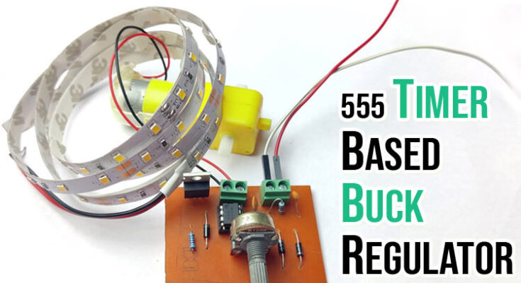
This article will demonstrate how to create a buck converter that can be used as a motor speed controller circuit or an LED dimmer circuit by utilizing an IRFZ44N N channel MOSFET and a 555 timer IC. This circuit is essentially a straightforward DC-DC Buck converter for power electronics that can be used to step down voltage. Because of its efficiency, which lowers heat generation and prolongs battery life, it is a good choice for tiny devices. I used KiCAD to design a converter circuit, built a straightforward internal PCB, and used an LED strip to test the module.
What distinguishes a buck converter from a linear voltage regulator, and what makes it more effective?
Both linear regulators and buck converters are step-down converters, meaning that the output
voltage is less than what was input. While the linear regulator continuously maintains the voltage divider network to maintain a constant output, the drawback of the linear regulator is that it wastes energy as heat in order to maintain the output. Buck converters use PWM switching to step down the voltage.
Theoretically, a buck converter is 100% efficient since it uses a PWM signal to maintain voltage; but, in practice, depending on the input and output voltages, these buck converters can be 90–95% efficient, while linear voltage regulators are quite inefficient. Therefore, because of its increased efficiency, a buck converter makes more sense if you are creating a small battery-operated system. The following table illustrates the distinctions between switching buck regulators and linear regulators.
| Buck converter | Linear Regulators | |
| Efficiency | High | Low |
| Complexity | Higher compared to linear voltage regulator | Lower than Buck converters |
| Size | Bigger compared to linear voltage regulator | Smaller than Buck converters |
| Range | Very high (from few milliwatt to 100s of kilowatt) | Low (few milli watt to few watts) |
| Cost | lower than Linear voltage regulators | Lower than Buck converters |
How are Buck converters operated?
To maintain the necessary output voltage, a basic buck converter simply opens and closes the switch during a predetermined duty cycle. An inductor to lessen changes in the output load, a capacitor to smooth out the output, a voltage source to supply the input voltage, a switch to maintain the duty cycle, and a diode connected in parallel to protect the switch—typically a transistor—from reverse voltage are the components of a simple Buck converter topology, as shown in the figure below.
Stage 1: When switch is closed

The inductor receives current from the input when the switch is closed. Because the inductor prevents abrupt changes in current, the current flowing through it is transformed into a magnetic field, which causes the inductor to begin charging. As a result, the capacitor also retains the charge when the switch is closed.
Stage 2: When the switch is open
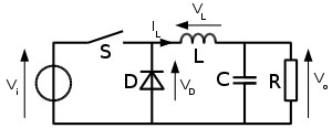
At this point, the switch is off, the inductor is not receiving any current, and it is functioning as a supply. The capacitor also helps to stabilize the output when the inductor loses energy. When the switch is closed once more, the procedure is repeated.
By adjusting the duty cycle, we can obtain any output voltage between 0 and the input voltage.
PWM output in use for our task. The passive and active parts that are attached to the IC 555 enable it to produce a frequency of about 30 KHz. The NE555 wiring diagram is provided below.
Converting Dollars Ssing a 555 Timer
We must turn on and off the switch far more quickly than a human can in order for the system to function in a real-world setting. Therefore, to complete the task, we employ a transistor as a switch and a PWM pulse generator. The output can be produced by an astable 555 timer integrated circuit.

How to Determine the 555 Timer’s PWM Frequency and Duty Cycle Formula
We utilized the IC 555 timer in astable mode to create the circuit. In this case, the output pulse alternates between high and low states continually. We can adjust the values of the resistor and capacitor (RC) network, which is coupled to the 555 timer, to alter the oscillation’s frequency. The following formula was used to select the values mentioned above for our circuit:
ON time (sec) = 0.693 * (R1 + R2) * C
OFF time (sec) = 0.693 * R2 * C
Frequency = 1.44 / ((R1 + R2 + R2) * C)
Duty cycle D = PW/T,
In this case,
T is the signal’s total period, D is its duty cycle, PW is its pulse width (or pulse active time), and all resistor and capacitor values are expressed in Farads and Ohms, respectively.

The waveform at various duty cycles is displayed in the image above. It is simple to conclude that a higher duty cycle indicates longer device energization times.
Buck Regulator Circuit Diagram Based on 555 Timer
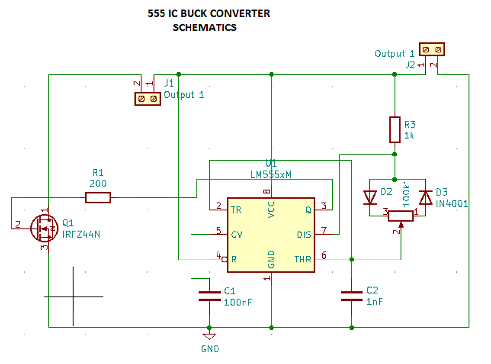
I created a preliminary circuit design on paper, using the aforementioned formulas to calculate the components, then chose the components based on the results. The 555 Timer-based Buck Regulator circuit is displayed below:
Components Needed for our Project:
- 1 x NE555
- 1 x IRFZ44N – N Channel mosfet
- 1 x 200 R, Resistor
- 1 x 1K, Resistor
- 3 x IN4001 Diode
- 1 x 100nF, Capacitor
- 1 x 1nF Capacitor
- 1 x 100k potentiometer
- 2 x 2pin connector
The circuit uses the 555 IC as the PWM generator and hence the whole circuit is based around the same. The connections of all 8 pins are mentioned below.
- Pin 1 is connected to the ground rail.
- Pin 2 and pin 6, with the ground through a 1nF capacitor.
- Pin 3 is connected to the gate of the mosfet. This pin sends the pwm output to the gate of the MOSFET.
- Pin 4 is connected to the +ve input rail.
- Pin 5 is connected to the ground with a 100nF capacitor. It helps in stabilizing the output and provide immunity against electrical noises.
- Pin 7 is connected to the +ve input with a 1k resistor and is also connected to the inverted diode setup.
- Pin 8 is connected to the +ve rail.
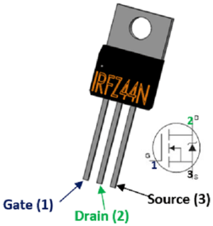
n the circuit above, the N-channel MOSFET, IRFZ44N is used as a switch, driven by the faint signal from IC 555. The Drain of this Mosfet is providing the negative switching control to the circuit. It has the following specifications.
- VDSS = 55V
- RDS(on) = 17.5mΩ
- ID = 49A
Constructing and Examining Our Buck Regulator System
I created the schematics using KiCad. The screen grab of the KiCad can be seen in the attached image below. Following the schematic design process, we allocated each component the correct footprint and placed the parts in the PCB designer tool. To etch the PCB, the design needed to be printed out once all the components had been arranged satisfactorily.

The picture below provides a step-by-step breakdown of the PCB manufacturing and testing process. If you would like to create this PCB yourself, you can also have a look at the page on making homemade PCBs. You can obtain the gerber file used for this project by clicking the link below.
